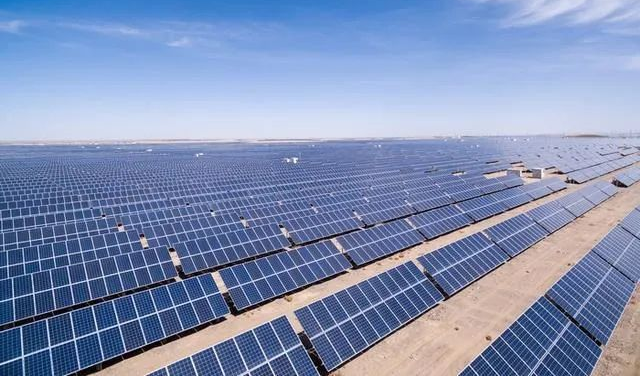
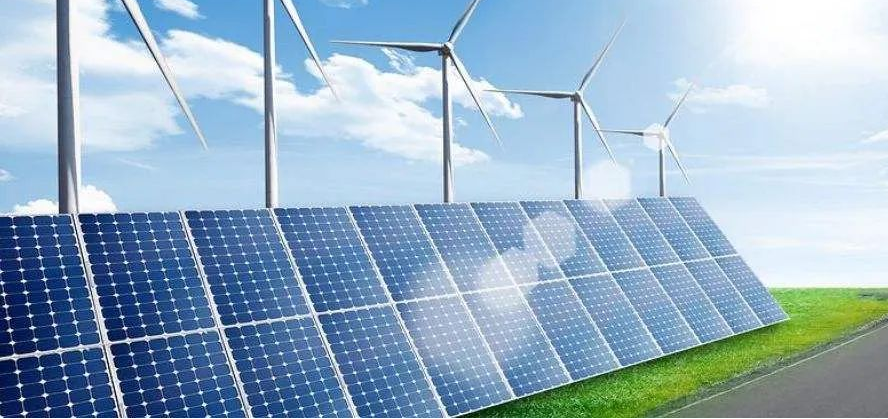
In May 2022, CCTV reported that the latest data from the National Energy Administration shows that as of now, the photovoltaic power generation projects under construction are 121 million kilowatts, and it is expected that the annual photovoltaic power generation will be newly connected to the grid by 108 million kilowatts, an increase of 95.9% over the previous year.
The continuous increase of global PV installed capacity has accelerated the application of laser processing technology in the photovoltaic industry. The continuous improvement of laser processing technology has also improved the utilization efficiency of photovoltaic energy. According to relevant statistics, the global PV new installed capacity market has reached 130GW in 2020, breaking a new historical high. While the global PV installed capacity has reached a new high, as a large all-round production country, China’s PV installed capacity has always maintained an upward trend. Since 2010, the output of photovoltaic cells in China has exceeded 50% of the global total output, which is a real sense. More than half of the world’s photovoltaic industry is produced and exported.
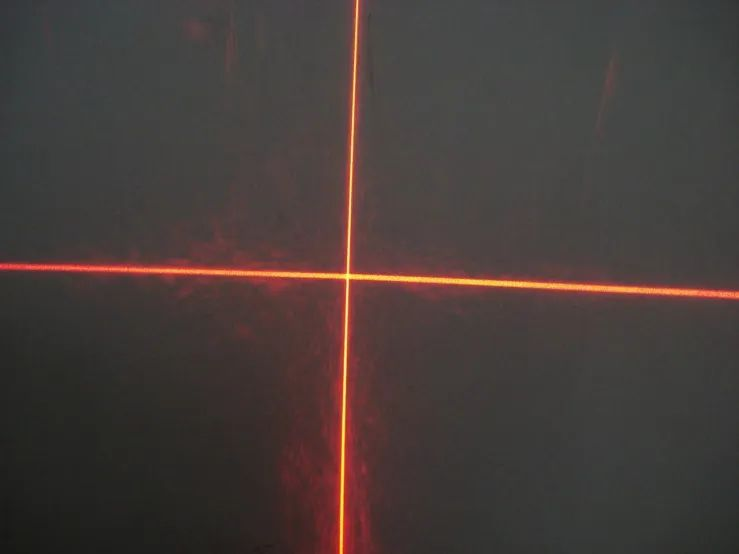
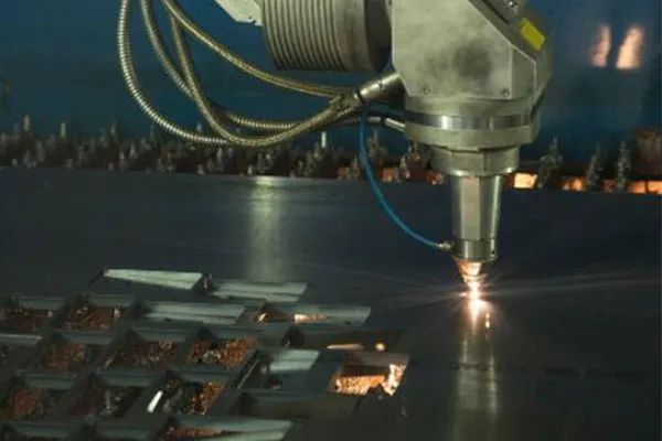
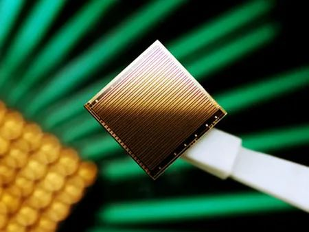
As an industrial tool, laser is a key technology in photovoltaic industry. Laser can concentrate a large amount of energy into a small area of cross section and release it, greatly improving the efficiency of energy utilization, so that it can cut hard materials. Battery manufacturing is more important in photovoltaic production. Silicon cells play an important role in photovoltaic power generation, whether crystalline silicon cells or thin film silicon cells. In crystalline silicon cells, high-purity single crystal/polycrystal is cut into silicon wafers for batteries, and laser is used to better cut, shape, and scribe, and then string the cells.
01 Battery edge passivation treatment
The key factor to improve the efficiency of solar cells is to minimize the energy loss through electrical insulation, usually by etching and passivating the edges of silicon chips. The traditional process uses plasma to treat the edge insulation, but the etching chemicals used are expensive and harmful to the environment. Laser with high energy and high power can quickly passivate the edge of the cell and prevent excessive power loss. With the laser formed groove, the energy loss caused by the leakage current of the solar cell is greatly reduced, from 10-15% of the loss caused by the traditional chemical etching process to 2-3% of the loss caused by the laser technology.
02 Arrange and Scribing
Arranging silicon wafers by laser is a common online process for automatic series welding of solar cells. Connecting the solar cells in this way reduces the storage cost and makes the battery strings of each module more orderly and compact.
03 Cutting and scribing
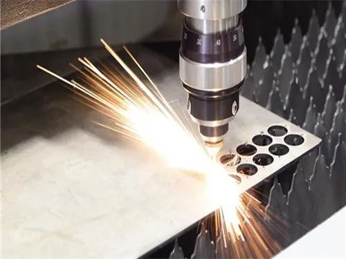
At present, it is more advanced to use laser to scratch and cut silicon wafers. It has high use accuracy, high repetition accuracy, stable operation, fast speed, simple operation and convenient maintenance.
04 Silicon wafer marking
The remarkable application of laser in silicon photovoltaic industry is to mark silicon without affecting its conductivity. Wafer labeling helps manufacturers follow up their solar supply chain and ensure stable quality.
05 Film ablation
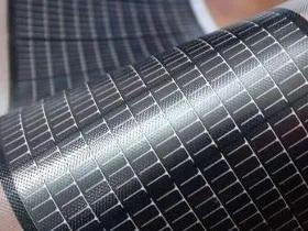
Thin film solar cells rely on vapor deposition and scribing technology to selectively ablate certain layers to achieve electrical isolation. Each layer of the film needs to be deposited rapidly without affecting other layers of the substrate glass and silicon. Instantaneous ablation will lead to circuit damage on the glass and silicon layers, which will lead to battery failure.
In order to ensure the stability, quality and uniformity of power generation performance between components, the laser beam power must be carefully adjusted for the manufacturing workshop. If the laser power cannot reach a certain level, the scribing process cannot be completed. Similarly, the beam must keep the power within a narrow range and ensure a 7 * 24 hour working condition in the assembly line. All these factors put forward very strict requirements for laser specifications, and complex monitoring devices must be used to ensure peak operation.
Manufacturers use beam power measurement to customize the laser and adjust it to meet the application requirements. For high-power lasers, there are many different power measurement tools, and high-power detectors can break the limit of lasers under special circumstances; Lasers used in glass cutting or other deposition applications require attention to the fine characteristics of the beam, not power.
When thin film photovoltaic is used to ablate electronic materials, the beam characteristics are more important than the original power. Size, shape and strength play an important role in preventing leakage current of module battery. The laser beam that ablates the deposited photovoltaic material onto the basic glass plate also needs fine adjustment. As a good contact point for manufacturing battery circuits, the beam must meet all standards. Only high-quality beams with high repeatability can correctly ablate the circuit without damaging the glass below. In this case, a thermoelectric detector capable of measuring laser beam energy repeatedly is usually required.
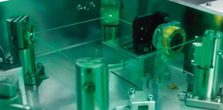
The size of the laser beam center will affect its ablation mode and location. The roundness (or ovality) of the beam will affect the scribe line projected on the solar module. If the scribing is uneven, the inconsistent beam ellipticity will cause defects in the solar module. The shape of the whole beam also affects the effectiveness of the silicon doped structure. For researchers, it is important to select a laser with good quality, regardless of processing speed and cost. However, for production, mode locked lasers are usually used for short pulses needed for evaporation in battery manufacturing.
New materials such as perovskite provide a cheaper and completely different manufacturing process from traditional crystalline silicon batteries. One of the great advantages of perovskite is that it can reduce the impact of processing and manufacturing of crystalline silicon on the environment while maintaining efficiency. At present, the vapor deposition of its materials also uses laser processing technology. Therefore, in the photovoltaic industry, laser technology is increasingly used in the doping process. Photovoltaic lasers are used in various production processes. In the production of crystalline silicon solar cells, laser technology is used to cut silicon chips and edge insulation. The doping of the battery edge is to prevent short circuit of the front electrode and back electrode. In this application, laser technology has completely surpassed other traditional processes. It is believed that there will be more and more applications of laser technology in the whole photovoltaic related industry in the future.
Post time: Oct-14-2022


